
Products
MAG*I*CAL
- Apertures
- Apertures 1,85 x 0,1mm
- Apertures 2,0 x 0,1mm
- Apertures 2,0 x 0,25mm
- Apertures 2,0 x 0,6mm
- Apertures 3,0 x 0,1mm
- Apertures 3,0 x 0,25mm
- Apertures 3,04 x 0,25mm
- Apertures 4,0 x 0,2mm
- Apertures 4,0 x 0,6mm
- Apertures 6.35 x 0.02mm
- Apertures 6,35 x 0,125mm
- Apertures 10,0 x 0,1mm
- Apertures 10,0 x 0,6mm
- Apertures 12,0 x 0,1mm
- Apertures 19,99 x 0,25mm
- Gilded strip apertures
- Multihole Strip Apertures
- Spray Apertures
- Thin Foil Apertures
- Tantalum Wehnelt
- Top Hat Apertures
- Aperture Cleaning
- Brushes
- Calibration
- GSR & Particle Analysis
- Light Microscopy
- SEM Calibration
- (CD) Calibration Test
- Back Scattered Electron Test
- Boron substrates
- Chessy test specimen
- Critical Dimension Magnification Standards
- Demonstration Specimens
- Glass size standards
- Gold on Carbon
- Gold Spheres on Carbon
- Line/Grid Standards
- Low & Medium Magnification
- MRS-3
- MRS-4
- MRS-6
- Multi Calibration Standard
- Polystyrene Spheres
- Silicon test specimen
- Tin on Carbon
- TEM Calibration
- Chemicals
- Cleaning
- Cryo Products
- Desiccators Cabinets
- Diamond Knives
- Dissection
- Embedding
- FIB Supplies
- Filaments
- Forensics
- General Lab Supplies
- Applicator, Sticks and Swabs
- Beakers, Cylinders and Containers
- Cell Strainer System
- Dishes and Boats
- Glass Bottom Dishes
- Laboratory Glassware
- Laboratory Tongs
- Microscopy Illuminators
- Microwave Specimen Holders
- Parafilm M®, Melinex Film
- PELCO Rotators
- Petri Dishes
- Pocket Scales
- Spatulas & Spoons
- Storage Jars, Containers & Bottles
- Thermometers
- Timers
- Ultraviolet Lamps
- Vials, Tubes and Cups
- Wire Mesh
- Gloves
- Grids
- Histology
- Immersion Oils
- Laboratory Tape
- Microscope Slides
- Pipettes and Pipettors
- PTFE Laboratory Products
- Razor- Microtome Blades
- Safety Products
- Slide Boxes, Trays & Mailers
- Slide Labels
- Spatulas and Spoons
- Staining
- Weighing Dishes
- Carbon tabs, tapes & sheets
- Mount Storage Boxes
- Planchets
- Replication Materials
- Scintillators
- Specimen Mount Grippers
- Specimen Preparation Stations
- Starter Kits
- Stubs, Mounts and Holders
- M4 Threaded, Cylinder, and Other Stubs
- Bulk Specimen Holders, M4
- Carbon Planchet Holders, M4
- Carbon, Brass, and Copper Mounts
- Cross Section Holders
- Cylinder Specimen Mounts
- E-Beam Lithography Mount, M4
- EBSD Pre-tilt Holders & Mounts, M4
- Filter Holders, M4
- Flat Sample Clip Holders
- Hitachi T-base Specimen Holders
- Metallographic Mount Holders
- Modular Stage Adapters, M4
- Mount Adapters, M4
- Multipurpose Specimen Holder
- Pin Stub Holders, M4
- Q Pin Mounts and Holders
- Rectangular Mounts
- SEMClamp Holders, M4
- SEMClip Cylinder Mounts
- SEMClip Geological
- STEM Imaging Holder, M4
- TEM Grid Holder, M4
- Tilt Specimen Holders
- Vise Type Holders
- Wafer & Large Sample Holders
- Pin Stubs Specimen Mounts and Holders
- Adapter Buttons
- Angled Pin Stub Holders
- Bulk Specimen Holders with Pin
- Carbon, Brass, and Copper, SEM Mounts
- E-Beam Lithography Mount
- EBSD Pre-tilt Holders & Mounts
- FIB Grid Holders
- Filter Holders, Pin
- Jeol Specimen Holders
- Low Profile FIB Mounts
- Low Profile SEMClip
- Metallographic Mount Holders
- Modular Stage Adapters
- Mount Adapters
- Multi Purpose / Bulk Holders
- Multi-Pin Stub Holders
- Pin Stub Specimen mounts
- Planchet Holders
- Q Pin Stubs and Holders
- Sample Holder Sets
- SEMClamp Holders
- SEMClip Pin Mounts
- Slotted Pin Stubs
- STEM Imaging Holder
- TEM Grid Holders
- Thin Section Holders
- Variable Tilt Holders
- Vise Clamp Holders
- Wafer Holders with Pin
- M4 Threaded, Cylinder, and Other Stubs
- Cabinets for Tissue Cassettes
- Cardboard, Tin Boxes & Cans
- Gel-Pak® Substrate Carriers
- Grid Storage Boxes
- Compact Modular Cabinet
- Plastic Jars, Containers & Bottles
- Membrane Boxes
- Plastic Storage Boxes
- Slide Boxes, Trays and Mailers
- Mount Storage Boxes
- Wafer Carrier Trays
- PELCO X-TREME Cases
- Zipper, Barrier Bags
- Accessories
- Aesculap® – Forceps
- Aquarius Tweezers
- Cantilever Tweezers
- Carbon Fibre tweezers
- Dumont™ Tweezers
- General Purpose Forceps
- Industrial, Economy Tweezers
- Mount Grippers
- PELCO Tweezers
- Plastic Tipped ESD Tweezers
- Plastic Tweezers, Flat & Sharp
- Plastic, Wafer Tip Styles
- Surgical Tissue Forceps
- Wafer Tweezers
- Wafer, Component, Cover Glass
- Wire Cutting Tweezers
- Zirconia Ceramic Tweezers
MAG*I*CAL®
Traceable Transmission Electron Microscopy Calibration Standard
The MAG*I*CAL performs all major TEM calibrations:
- All TEM magnification ranges
- Camera constant
- Image Diffraction Pattern Rotation
- Directly traceable to a natural constant
MAG*I*CAL® is the world’s smallest ruler and have been inducted into the Guinness Book of World Records.
In the diagrams of the MAG*I*CAL® grid located above, the arrows point to the four regions containing the calibration marks.
MAGNIFICATION CALIBRATION STANDARD FOR TEM
MAG*I*CAL™ consists of an ion milled cross section of a silicon single crystal consisting of a series of atomically flat layers of Si and SiGe, which have been grown epitaxially by MBE (molecular beam epitaxy).
When the calibration structure is viewed in a TEM, it appears as a series of light and dark layers where the layer thicknesses are accurately known.
The calibra- ted thickness measurements of these light (silicon) and dark (SiGe) layers are based on careful TEM measurements of the <111> lattice spacing of silicon, which is visible on the calibration sample itself, and are supported by x-ray diffraction measurements.
The layer spacing are designed so that the sample can be used to calibrate the entire magnification range in a TEM, from 1,000X to 1,000,000X. As the sample is also a single crystal of silicon, the calibrations requiringelectron diffraction information such as the
came- ra constant and image/diffraction patternrotation can also be performed easily andunambiguously.
One single calibration sample can therefore be used to provide all three of the major TEM instrument calibra- tion at all magnifications and all camera lengths.

To improve accuracy when making measurements, always measure the largest distance clearly visible on the micrograph.
For example, at the highest magnification ranges, measure the distance across the entire set of five dark layers and four light layers, instead of trying to measure an individual dark layer.
Aligning the Reference Standard
The MAG*I*CAL ™ Calibration Standard is made from a single crystal of silicon, and therefore has many very useful attributes as a TEM standard.
To take advantage of these attributes, mount the standard in the TEM sample holder with the epoxy line of the standard parallel to the stem of the TEM sample holder (see Fig.2, next page).
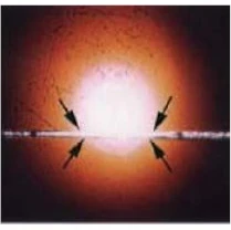
Translate the standard to bring into view the calibration marks close to the thin edge near the perforation in the center of the sample (arrows, Fig. 2), and focus. Put the TEM into diffraction mode, choose the smallest camera length, and adjust the intensity control (condenser control) back and forth to find the proper value of over-focus that forms the striking pattern called a Kikuchi pattern, similar to Fig. 1 below, but perhaps rotated.
These Kikuchi bands are formed by elastic Bragg scattering of previously inelastically scattered electrons. The intensity control can be adjusted so that either a diffraction spot pattern or a Kikuchi pattern can be observed.
The standard should be tilted to move the Kikuchi pattern so that the central “intersection” in this diagram (where the largest number of bands intersect) is centered on the brightest (zero order) diffraction spot in the electron diffraction pattern (adjust the intensity control back and forth).
It may be necessary to translate the standard to slightly thicker or thinner regions to get a clear Kikuchi pattern.
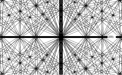
Kikuchi pattern of single crystal silicon viewed down the zone axis. The broad horizontal band in the center of this figure is between the {200} Kikuchi lines.
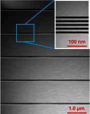
TEM micrograph of the MAG*I*CAL®. Inset shows a higher magnification image of one of the layered structures
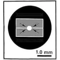
Diagram of the MAG*I*CAL® grid. The arrows point to the four regions containing the calibration marks.
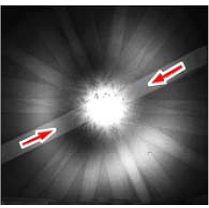
A Kikuchi pattern from the single crystal sample which can be used to align the sample.
An optical micrograph of the colors of silicon when it is thinned down to TEM thicknesses, the 1mm central perforation, and the four areas containing the calibration markings (arrows).
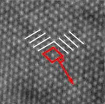
A lattice image of the single crystal silicon sample. The silicon lattice planes should be measured perpendicular to the planes, in the direction of the arrow.

| Art. | Description | Unit | Price | Quantity | |
|---|---|---|---|---|---|
| S1936 | MAG*I*CAL Calibration Standard | Each | € 2.004,10 |