
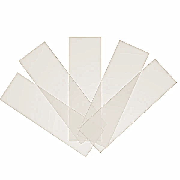
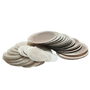
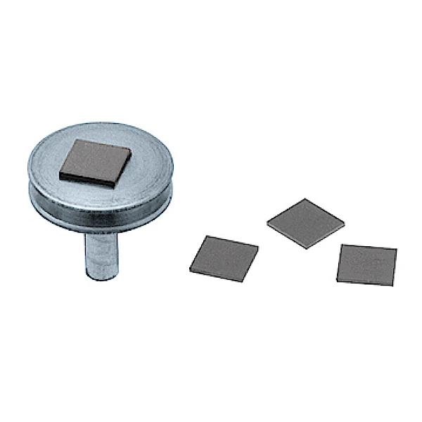
Highest Grade Mica Sheets
Highest quality Grade V1
0.15 to 0.177mm thick
Sheets interleaved
Various sizes
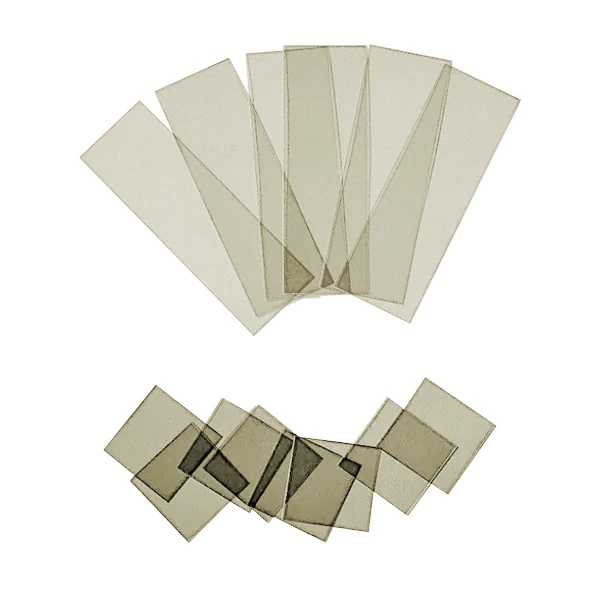
Hi-Grade Mica
Grade V2
0.23 to 0.3mm thick
Sheets interleaved
Various sizes
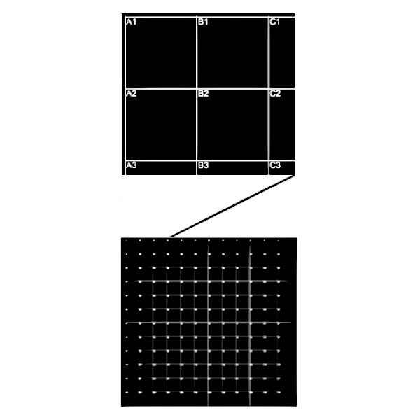
Pelcotec SFG12 Finder Grid Substrate
The innovative Pelcotec SFG12 finder grid substrate is a flat, conductive silicon substrate with a die size of 12.5 x 12.5mm.
It is covered with a 1 x 1mm raster giving a total of 12×12=144 fields.
Each field has a unique label using an alphanumeric pattern.
The lines and labels are precision laser etched in the silicon surface. It is the best combination of a flat specimen support and an SEM finder grid.
This unique and innovative product has some resemblance with an engraved SEM specimen mount, but it has a number of additional advantages:
- Flat – there are no height differences like with copper finder grids
- Fine pattern over a large area – better defined than engraved SEM mounts
- Low background signal – same as with Si chip substrates
- For EDX analysis only one element (Si) from the finder substrate
- Practical and easy to navigate – 1mm spacing with 144 fields
- Pattern is visible with naked eye, preparation microscope and SEM
- Gives an approximate size at (very) low magnification
- Can easily be mounted on SEM sample stubs – compatible with most popular sizes
- Can be used with SEM, FIB, XPS/ESCA, Auger and LM
Specifications of the silicon substrate used: prime virgin silicon wafer, P Boron doped, <100> orientation, resistivity of 0.5-35 ohm/cm, thickness 645 m 55 m.
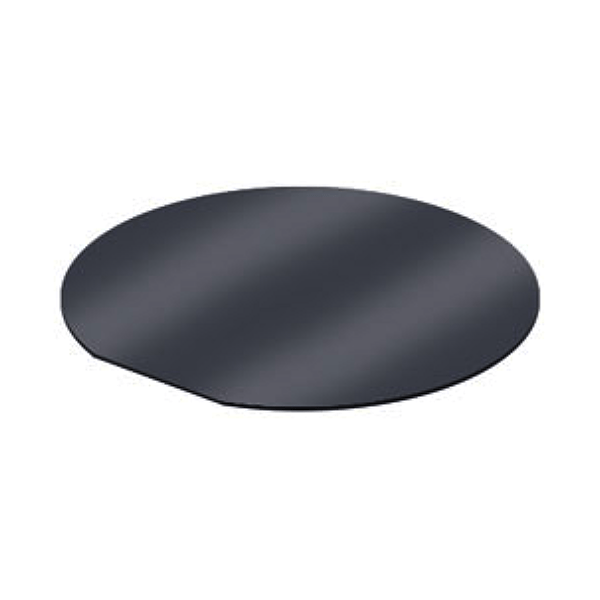
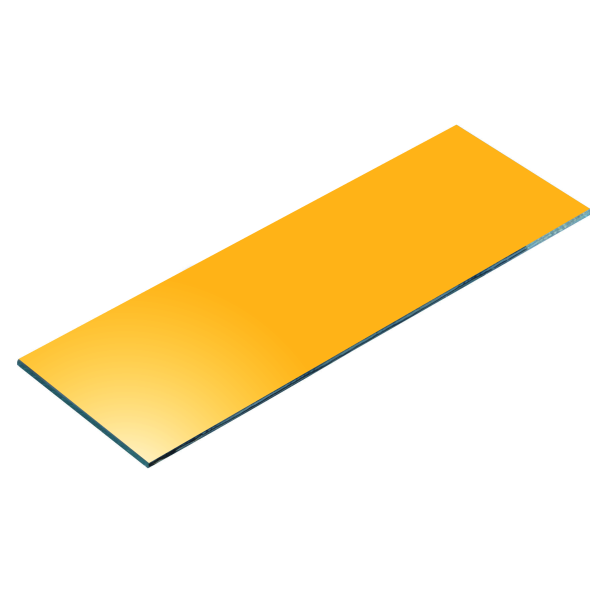
PELCO Mica Sheets, Grade V5
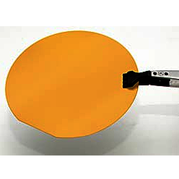
Various sizes available, presenting many fresh, clean surfaces for such EM applications as carbon filming and particle spraying.
Thickness, 0.23mm – 0.3mm
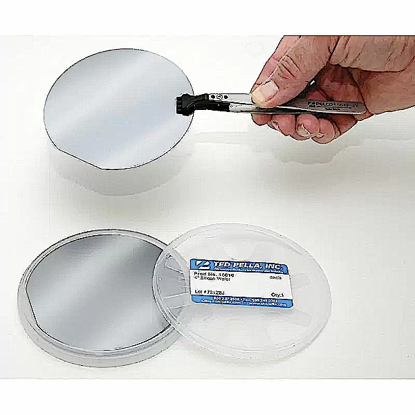
hese 1″, 2″, 3″, 4″ and 6″ (25.4, 50.8, 76.2, 100, 150mm) diameter silicon wafers can be used either as a substrate for thin film research or to make smaller substrates by dicing the wafer into pieces using Scribing and Cleaving Kits and hand tools. The wafer is shipped in a coin-style wafer carrier.
Properties:
- Orientation: <100> for 1″, 2″, 3″, 4″ and 6″ wafer <111> for 3″ P type
- Resistivity: 1-50 Ohm-cm
- Type P: (Boron) (1 primary flat)
- Type N: Phosphorous doped (1 primary flat)
- No SiO2 top coating
- Wafer thickness:
Ø1″ = 0.010 – 0.012″ (275 – 325µm)
Ø2″ = 0.010 – 0.012″(255 – 305µm)
Ø3″ = 0.013 – 0.017″ (330 – 420µm)
Ø4″ = 0.020 – 0.021″ (505 – 545µm)
Ø6″ = 0.023 – 0.027″ (585 – 695µm)
- Roughness: 2nm
- TTV: ≤5µm
- Bow/Warp: ≤30µm
- Wafer is polished on one side, etched on the other
AFM Mica Discs
Highest quality grade V1 mica, 0.21mm (0.0085 ) thick. Interleaved, in packages of 10. Can be mounted on AFM/STM discs.
Available in four diameters:
10mm
12mm
15mm
20mm
Ultra-Flat 6″ Silicon Wafers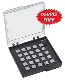
Ultra-Flat 6″ diameter Silicon Wafer for demanding substrate studies. The 6″ ultra-flat silicon wafer is shipped in a 6″ Wafer Carrier.
Also available as 5 x 5mm, 5 x 7mm, 10 x10mm stealth-diced dies in Gel-Pak® boxes. Stealth dicing eliminates edge-chipping and cutting debris associated with saw dicing, providing the cleanest, most uniform product possible.
All products are packed in class 10 clean room conditions.
Properties for 6″ (150mm) Ultra-Flat Wafer:
- Material: CZ Virgin Silicon Wafer
- Grade: Prime
- Diameter: 150mm
- Orientation: <100>
- Type/Dopant: P/Boron
- Resistivity: 10-20 ohm-cm
- Thickness: 675µm +/- 20µm
- TTV: ≤2µm
- Site Flatness: <=1µm
- Warp: ≤30µm
- Bow: ≤20µm
- Particles: ≤30@≥0.2µm
- Front Surface: Polished
- Back Surface: Etched
- Flat: 1 per SEMI Standard
| Ultra-Flat Thermal SiO2 Substrates The Ultra-Flat SiO2 substrates consist of a 200nm thermally grown amorphous SiO2 film on an ultra-flat silicon wafer.SiO2 is one of the most characterized materials and is widely used in semiconductor manufacturing, thin film research and as substrate for growing cells.It can be directly used as substrate for AFM and SEM imaging.The ultra-flat thermal silicon dioxide substrates are available in 6″ wafer and conveniently diced 5 x 5mm, 5 x 7mm and 10 x 10mm chips.The 6″ wafer is shipped in a 6″ wafer carrier, the diced pieces are shipped in a Gel-Pak box.The special clean dicing process involves coating the wafer with photo resist before dicing and removing it after dicing which produces debris-free SiO2 substratres.All products are packed in class 10 clean room conditions.Properties for thermal SiO2 substrates:
|
 |
|
| Ultra-Flat Thermal 6″ SiO2 Wafer | ||
 |
||
| 5 x 5mm Diced Ultra-flat Thermal SiO2 Substrates |
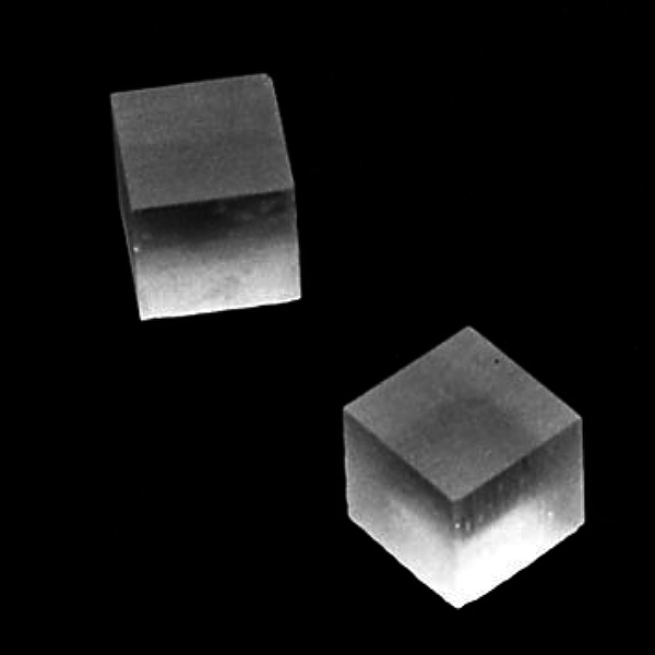
Single Crystal Substrates (NaCl, KBr and KCl)
High purity, optical grade single crystals of sodium chloride (NaCl) MSDS, potassium bromide (KBr) and potassium chloride (KCl) form excellent substrates to grow epitaxial films.
The orientation of the vacuum coated thin films is directly related to the orientation of the single crystal substrate thereby creating single crystal films.
Ideal for thin film research, education and studies of properties of single crystal films.
Impurities are less than 1%.
All three materials are supplied with (100) orientation with a crystal size of 10 x 10 x 10mm in packs of 5.
For most applications it is advisable to use freshly cleaved substrates.
The cleaved surfaces produce atomically flat areas; however, cleavage steps over different atomic planes should be expected.
PELCO Quartz Glass Substrate Discs
The PELCO Quartz Glass Discs or Wafers are made from high quality fused quartz (glassy, amorphous material – not a single crystal) (Technical Data on GE 124 Quartz) ground and optical-grade clear polished on both sides.
The discs are ideal as substrates for thin film research and are also suitable for optical research.
These quartz wafers have excellent chemical resistance against a wide variety of solvents.
They have also excellent heat resistance with high dimensional stability over a wide temperature range.
Transparency is provided for 0.19 to 4.2 m with very low absorbance in the 0.26 to 2.6 m range.
Surface flatness is 1 degree with 60/40 scratch/dig specifications.
Available in sizes from 1″ to 4″ diameter with thickness of 1/16″ and 1/8″.
PELCO Sapphire Substrate Discs
The PELCO Sapphire Discs or Wafers are made from high purity clear sapphire (Al2O3), ground and optically clear polished on both sides.
Sapphire has a wide transmission range; from 150 to 6000nm with low absorbance in the 300 to 4500nm range.
The discs are ideal as substrates for thin film research and are suitable for optical research.
Excellent resistance against a wide range of chemicals. Surface polish to one microinch or better on each face.
Tolerances are 0.001″ (0.025mm) in diameter and thickness; flatness to 0.0003″ (0.0008mm) or better.
Available in 0.5″ (12.7mm), 0.75″ (19mm) and 1″ (25.4mm) diameter with a choice of thickness between 0.010″ or 0.125″ (0.25 or 3.2mm).
PELCO Gold Coated Silicon Wafers
2″ and 4″ gold coated silicon wafers, useful for a variety of applications such as SEM or AFM supports, nanotechnology and biotechnology.
Both Cr and Au are evaporated on the silicon wafers using a vacuum evaporation system with chromium between the glass and the gold to serve as an adhesion layer.
The gold surface is not atomically flat, but has bumps in the nm range.
The wafers are packed and shipped in a wafer carrier.
Au coating should be stable to about 175 C; above that temperature delamination could occur.
Specifications:
- Wafer: thickness 4 , 460 – 530 m, 2 , 254 301 m, <111> orientation, P-type
- Chromium adhesion layer thickness: 5nm
- Gold layer thickness: 50nm ( 5nm)
- Diameter: 2″ or 4″
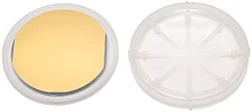 |
| 2″ Gold Coated Silicon Wafer in wafer carrier |
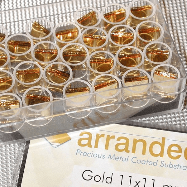
Arrandee gold-coated substrates
Arrandee gold-coated substrates use a borosilicate glass base of 0.7mm thickness.
They are suitable for easy preparation of gold terraces and by simple flame annealing 100 x 100 nm Au (111) terraces can easily be obtained.
A thin layer of chromium, 1 to 4 nm, is applied to the glass surface. This layer guarantees optimum adhesion to the glass as well as to the subsequently deposited gold layer (250 nm 50nm).
Arrandee substrates are very useful for SPM investigations.
Si-chips are opaque, of low electrical resistance and have surface properties equal to glass (including smoothness). They are also good substrates for growing or mounting cells. Si-chips are precleaned before packaging. Also ideal for imaging small particles due to low background signal.
Availability: 4″ wafer (#16010) is precut into 5 x 7mmm, 5 x 5mm, 10 x 10mm, 20 x 20 mm or 20 x 30mm chips that can be easily separated in the laboratory.
- 4″ wafer precut into 5 x 7mm chips approximately 187 chips/wafer
- 4″ wafer precut into 5 x 5mm chips approximately 270 chips/wafer
- 4″ wafer precut into 10 x 10mm chips approximately 55 chips/wafer
- 4″ wafer precut into 20 x 20mm chips approximately 10 chips/wafer
- 4″ wafer precut into 20 x 30mm chips approximately 6 chips/wafer
PELCO Gold Coated Microscope Slide
High quality glass, standard microscope slides coated with 50nm of gold with a 5nm chromium adhesion layer between the glass slide surface and the gold coating.
Can be used for a wide range of nanotechnology, biotechnology and AFM applications.
Also suitable as an opaque microscopy support.
Both Cr and Au are evaporated on the glass slide using a vacuum evaporation system.
The gold surface is not atomically flat, but has bumps in the nm range.
The gold slides are individually packed in a slide mailer. The gold slides are autoclavable.
Specifications:
- Glass slide: 75 x 25mm , 1mm thickness, soda lime glass
- Chromium adhesion layer thickness: 5nm
- Gold layer thickness: 50nm (+/- 5nm)
- Gold purity: 99.999%
PELCO Gold Coated Glass Coverslips
High quality, borosilicate glass coverslips coated with 50nm of gold with a 5nm chromium adhesion layer between the coverslip surface and the gold coating.
Can be used for a wide range of nanotechnology, biotechnology and AFM application.
Both Cr and Au are evaporated on the glass coverslips using a vacuum evaporation system.
The gold surface is not atomically flat, but has bumps in the nm range.
The coverslips are sold in packs of 2 and are packed in an X0 Gel-Pak box.
The gold coated coverslips are autoclavable.
Specifications:
- Glass coverslips size: 16mm with thickness #1 (0.13-0.16mm) or 22x22mm with thickness #2 (0.19-0.25mm)
- Glass type: Schott D263M borosilicate
- Chromium adhesion layer thickness: 5nm
- Gold substrate layer thickness: 50nm ( 5nm)
- Gold purity: 99.999%